
0.1uF DF value bad analysis
Release time:
2022-07-19
0.1μF/275V D2 DF high reason analysis Capacitors are one of the most heavily used components in electronic equipment, and the DF value is one of the four main parameters for measuring capacitor performance (capacity, DF, insulation, and voltage withstand), which directly leads to heat generation in the use of capacitors.
0.1μF/275V D2 DF high reason analysis
Capacitors are one of the most used components in electronic equipment, and the DF value is one of the four major parameters (capacity, DF, insulation, and voltage withstand) that measure the performance of capacitors, which directly leads to heat generation in the use of capacitors. When the heat generated inside the capacitor is greater than the heat emitted to the outside, the temperature inside the capacitor is getting higher and higher, which finally leads to the thermal breakdown of the capacitor. Therefore, the internal temperature of the capacitor rises in actual use due to the loss of the capacitor itself.
Metallised film capacitors are wound with metallised film, sprayed with metal on the end faces and soldered with leads, so the DF value becomes a key factor for quality control during the production process. The loss of metallised film capacitors mainly consists of the loss of the dielectric part and the metal part (pole plate, pole plate and gold sprayed layer, gold sprayed layer and leads, leads).
1, The loss of the medium part
Because this product is produced with polypropylene film, the dielectric loss is very small, so the high loss is mainly caused by the metal part.
2、 Losses in the metal part
Metallised film capacitor metal part of the loss by the capacitor's lead wire loss (CP line), CP line and gold spraying layer contact loss, gold spraying layer and the vegetal end face contact loss and pole plate loss together. It can be expressed by the following formula.
tgδ=tgδlead+tgδ1+tgδ2+tgδpole
Formula:
tgδ : Lead loss
tgδ1 : contact loss between CP wire and gold spray layer
tgδ2 : contact loss between the gold spray layer and the end surface of the prime
tgδPole: pole plate loss
2.1Lead loss
tgδ引 =wC*r引=2πfc*4/π*ρι/d2*kd
Formula:
ρ:Resistivity/Ω.cm; d:Diameter/ cm; ι:Length/ cm; k:Constant related to conductor material k=0.106 Our company uses tinned copper clad steel wire line, so the above equation is simplified as:
tgδ lead =0.85*ρι/d2*f*C
It can be seen that the loss is proportional to the length and inversely proportional to the diameter, when used at higher frequencies, the lead loss is not negligible part.
2.2 Plate loss
The schematic diagram of the pole plate of a metallised film capacitor is as follows.
Translated with www.DeepL.com/Translator (free version)
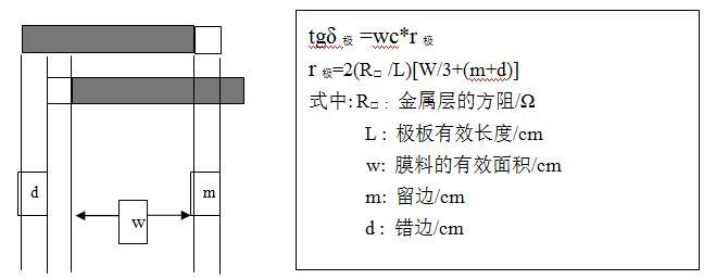
The reason for the increase of r-pole is the increase of R-pole of metallised film during processing, and the other reason is the increase of square resistance caused by the oxidation of the metal layer. Therefore, the tension should be even during the winding process of the prime, and the prime should not leave any gap to prevent the oxidation of the metal layer.
a) The contact loss between CP wire and gold spraying layer and the contact loss between gold spraying layer and the end surface of the prime mover.
In the case of good and outstanding soldering, the contact loss between CP wire and gold spray layer tgδ1 should be 0. As for the contact loss between the gold spray layer and the end face of the vegetal, the quality condition of the gold spray layer is very critical due to the existence of a certain contact resistance. The main reason for the increase of capacitor DF is also determined by this 2 contact points.
Output 2.1KV Storage 2.5KV Pulse test
一 Test Conditions
Temperature: 25℃ Apparatus: Pulse Tester Output Voltage: 2100Vdc
Humidity: 75% Expiry date: 2008/10/29 Storage voltage: 2500Vdc
Test Sample)
0.1UF/275V D2
|
Serial number |
Pre-test | Post-test | Value of change | Anatomy of a Suko | Gauge | ||||
|
Electrostatic capacity |
DF |
Electrostatic capacity |
DF |
% change in capacity |
Change in DF value |
OK& NG |
|||
|
1 |
100.460 |
1 |
97.553 |
3 |
-2.89% |
2 |
正常 |
OK |
|
|
2 |
100.870 |
1 |
100.950 |
1 |
0.08% |
0 |
正常 |
OK |
|
|
4 |
96.301 |
1 |
94.078 |
25 |
-2.31% |
24 |
端面凹陷 |
NG |
|
|
5 |
98.286 |
1 |
98.825 |
4 |
0.55% |
3 |
正常 |
OK |
|
|
6 |
97.608 |
2 |
98.267 |
8 |
0.68% |
6 |
正常 |
OK |
|
|
7 |
99.332 |
1 |
99.142 |
19 |
-0.19% |
19 |
焊接压力过大 |
NG |
|
|
8 |
97.202 |
1 |
97.193 |
2 |
-0.01% |
1 |
正常 |
OK |
|
|
9 |
98.886 |
1 |
99.318 |
2 |
0.44% |
1 |
正常 |
OK |
|
|
10 |
98.174 |
1 |
98.735 |
2 |
0.57% |
1 |
正常 |
OK |
|
Capacitor loss power p = V2 * W * C * tgδ It can be seen that in the case of the voltage, the power is unchanged tgδ increase will directly lead to the increase in the loss power of the container. Through the above analysis, it can be seen that improvement measures should be taken in the following aspects.
1. The end surface of the vein is flat, not concave & core pulling. 2.
2. Spraying operation is strictly based on SOP, and its parameters should not be changed arbitrarily. 3.
3. the excitation between the welding head is properly adjusted, the welding pressure is moderate. 4. the welding current should not be too large.
4. The welding current should not be too large, according to the SOP setting. Instantaneous current is too large will lead to close to the lead part of the vegetal end surface contraction, caused by the contact resistance increases, using short-circuit charging and discharging high-frequency (10KHz) can be rejected early failure of good products.
Reporter: Zheng Shikang
Tag:
Previous Page
Next Page
Previous Page:
Next page:
Share
Foshan Shunde Beijiao Huada Electric Appliance Industry Co., Ltd.

WeChat Public Number
Service Hotline
Company Address
No.16, Industrial Avenue, Beijiao Town, Shunde District, Foshan City, Guangdong Province
©All rights, Beijiao Huada Electric Appliance Industry Co., Ltd., Shunde District, Foshan City, 2022 reserved.Website Construction: Power of Chinese Enterprises Shunde seo tag